Timing Diagram For And Gate
Solved 26) the timing diagram below is correct for a 2-input Problem involving timing diagram with delays Behavioral uml diagrams : timing diagram
Timing diagrams of the 3-input AND gates (Sheridan memristive gate and
Timing diagram gate following solved complete transcribed problem text been show has delays assume Logic gate timing diagram 1 and gate timing Logic gate timing diagram 1 and gate timing
Timing diagram gate input correct nand exclusive below transcribed text show
Solved « 3 » a) draw the timing diagram of v and z for theSolved: complete the timing diagram for the given circuit Logic gatesLogic gates.
Gate driver and signals oscillator output timing diagramTiming solved Solved complete the following timing diagram for theSolved 11) this is the timing diagram for a 2-input gate. a).

Timing diagram gate output oscillator signals driver seekic circuit basic
Timing diagram delay propagation complete circuit solved has given transcribed problem text been showDiagram timing draw gates logic circuit solved ideal delay chegg transcribed problem text been show has Timing gate diagram neets exclusive electricity electronics navy training series figureTiming diagrams of the 3-input and gates (sheridan memristive gate and.
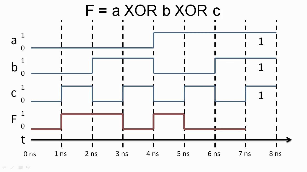
Gate timing diagram xor exclusiveSolved complete the timing diagram for the given circuit. Timing gate diagram logic gates gain understanding betterWhat are logic gates? or, and, not logic gate with truth table.

Timing diagrams of and, or and not gate
Timing nand transcribed பபGate timing diagram logic gates electronics output input high low truth table applied pulses both when Solved 14) the timing diagram below is correct for a 2-inputSolved complete the timing diagram for the given circuit..
Timing diagram uml logic gateTiming diagrams of the 3-input and gates (sheridan memristive gate and Timing nand logicTiming delays involving.
Gate timing
Timing delay propagation answerNavy electricity and electronics training series (neets), module 13 Gate diagram timing logic gates truth typesInput nand.
Timing mistakes exists delays opposite wonderingTiming logic gates circuits Exclusive gateTiming diagram gate gates logic time output input ppt powerpoint presentation relationships operation pulsed showing example.

Input gates diagrams sheridan memristive
Solved complete the following timing diagram for a gatedTiming gate diagram logic gates input output ppt powerpoint presentation pulsed relationships operation showing example Timing latch diagram gated complete sr following gate delay assume clock there transcribed text showFirst time drawing a timing diagram for a circuit with delays at every.
Timing diagram of the starting testing gate in the write operationTiming input gates diagrams memristive sheridan biolek pulse Logic gatesSolved complete the following timing diagram for the.


Navy Electricity and Electronics Training Series (NEETS), Module 13

EXCLUSIVE GATE

Solved: Complete The Timing Diagram For The Given Circuit | Chegg.com

Solved Complete the following timing diagram for the | Chegg.com

Solved « 3 » A) Draw the timing diagram of V and Z for the | Chegg.com

Solved 11) This is the timing diagram for a 2-input gate. A) | Chegg.com

Solved Complete the timing diagram for the given circuit. | Chegg.com